ON Semiconductor NB3N111KMNG
NB3N111KMNG, Clock Driver HCSL HCSL, LVDS, 32-Pin QFN
Mfr. Part #: NB3N111KMNG / RS Stock #: 70340311

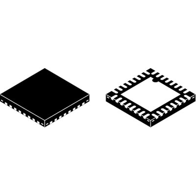
Image may be a representation. See specs for product details.

Price
Qty.
Standard Price
1
$10.49
5
$9.97
10
$9.44
20
$8.92
Additional Inventory
 Bulk pricing available
Product Specifications
Product Attribute
Attribute Value
Search
Dimensions
0.037\” (0.95mm) X 0.00 in W X 0.20 in L
Input Signal Type
HCSL ; LVCMOS ; LVDS ; LVPECL ; LVTTL
Logic Family
HCSL
Logic Function
Clock Driver
Logic Level
HCSL, LVDS
Maximum Operating Temperature
85 °C
Minimum Operating Temperature
-40 °C
Mounting Type
Surface Mount
Number of Clock Inputs
1
Number of Pins
32
Operating Voltage Range
3 to 3.6 V
Operation Mode
Differential, Single Ended
Package Type
QFN
Temperature Operating Range
-40 to +85 °C
Overview
The NB3N111K is a differential 1:10 Clock fanout buffer with High-speed Current Steering Logic (HCSL) outputs optimized for ultra low propagation delay variation. The NB3N111K is designed with PCI Express HCSL clock distribution and FBDIMM applications in mind.
Inputs can directly accept differential LVPECL, LVDS, and HCSL signals. Single-ended LVPECL, HCSL, LVCMOS, or LVTTL levels are accepted with a proper external Vth reference supply. Input pins incorporate separate internal 50 Ω termination resistors allowing additional single ended
system interconnect flexibility.
The NB3N111K specifically guarantees low output–to–output skew. Optimal design, layout, and processing minimize skew within a device and from device to device. System designers can take advantage of the NB3N111K’s performance to distribute low skew clocks across the backplane or the motherboard.
Features:
Typical Input Clock Frequency 100, 133, 166, or 400 MHz
220 ps Typical Rise and Fall Times
800 ps Typical Propagation Delay
tpd 100 ps Maximum Propagation Delay Variation per Diff Pair
0.1 ps Typical RMS Additive Phase Jitter
LVDS Output Levels Optional with Interface Termination
Operating Range: VCC = 3.0 V to 3.6 V with GND = 0 V
Typical HCSL Output Levels (700 mV Peak-to-Peak)
LVDS Output Levels with Interface Termination
These are Pb-Free Devices